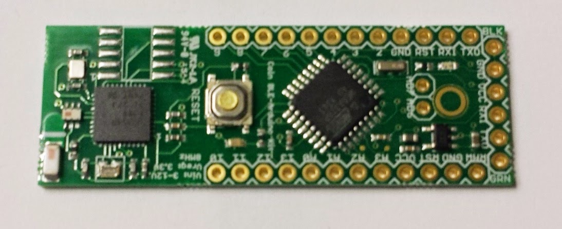
The following instructions are for setting up a brand new Coin BLE Dev Board for easy programming with the Arduino IDE and Bluetooth integration. Even though the original boards sold out and Coin did not plan on doing another manufacturing run, many people were still interested in getting their hands on these boards. Because of this, our team took over the second manufacturing run so that everyone who wants the board can get one.
To purchase your own Coin BLE Dev Board (NO LONGER AVAILABLE), visit http://coindev2.myshopify.com/
The boards come assembled fresh from the factory, so this post documents the steps that must be followed to get your board programming ready.
The original Coin BLE Wiki can be found at https://github.com/CoinApps/arduino-ble-dev-kit/wiki
To Program the BLE module:
- For default BLE behavior (send 1 byte at a time from the Arduino via Bluetooth) or if you do not want to write any custom code for the BLE module, program the out1-19-NOV-2013.hex file provided on the Coin Wiki (Git Hub Link to code)
- Follow the instructions to program the BLE module here: Coin Wiki for BLE Software Instructions
To Program the Bootloader on the Arduino
2 Methods:
- Using the Atmel mkII AVRISP Programmer
- Using another Arduino and the Arduino IDE
Method 1: Atmel mkII AVRISP Programmer
Requirements:
- 6 pin 0.1" male-to-male header

- Jumper wires
- Coin BLE Dev Board

- FTDI Programming Cable

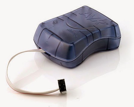
- Atmel mkII AVRISP Programmer (~$37.00)

- Atmel Studio 6 or Atmel Studio 6 Programmer Standalone (free software, download link here)
- Jumper wires
Instructions:
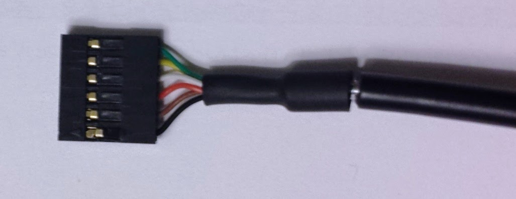
1) Place 6 pin header into the FTDI cable
2) Wire the following pins up to the mkII programmer (no need to solder them in, just bend to ensure pin contact)
 |
| ***Taken from http://www.avrfreaks.net/index.php?name=PNphpBB2&file=printview&t=81538 *** |
3) Place FTDI cable into dev board for powering the board (the red light will be on). Make sure you orient the FTDI cable correctly when you connect it (the board says GRN on the side that corresponds to the green wire on the FTDI cable)
4) Open up Atmel Studio 6: Tools >> Device Programming
5) When the programming window pops up, set up the following properties
- Tool: Select AVRISP mkII
- Device: ATA6614Q
6) Click Apply
7) IMPORTANT: Under the Interface Settings tab, set the ISP Clock to 125kHz (for the first time this must be done since the fuse settings haven't been set yet)
8) Under the Memories tab, browse for the ATmegaBOOT_168_atmega328_pro_8MHz.hex bootloader (under most normal Windows installs, this will be located under C:\Program Files (x86)\Arduino\hardware\arduino\bootloaders\atmega\)
9) Click Program
10) Upon success, go the the Fuses tab and set the fuses to the following:
- EXTENDED: 0xFD
- HIGH: 0XDA
- LOW: 0XFF
11) Click Program
12) Now verify that the bootloader was properly loaded by opening up the Arduino IDE and loading the "Blink.ino" file onto the dev board using the FTDI cable only as the following describes:
- Select the proper serial port where your FTDI programming cable is plugged into
- Under Board, select Arduino Pro or Pro Mini (3.3V, 8MHz) w/ATmega328
Method 2: Use another Arduino as a AVRISP programmer
The second method is to use another Arduino to program the bootloader. This can be done with the setup seen below, except for replacing the top Arduino with the dev kit board. Modified from http://arduino.cc/en/Tutorial/ArduinoToBreadboard.
If you have a new ATmega328 (or ATmega168), you'll need to burn the bootloader onto it. You can do this using an Arduino board as an in-system program (ISP). If the microcontroller already has the bootloader on it (e.g. because you took it out of an Arduino board or ordered an already-bootloadedATmega), you can skip this section.
To burn the bootloader, follow these steps:
- Upload the ArduinoISP sketch onto your Arduino board that you will be burning the bootloader from (You'll need to select the board and serial port from the Tools menu that correspond to your board.) This can be found in the Arduino IDE at File >> Examples >> ArduinoISP. Upload this sketch to the device.
- Wire up the Arduino board and microcontroller as shown below. The 4 yellow wires in the image from the programmer Arduino should instead be contacted with the following pins on the dev board (once again, just make sure you have contacts on the pins using the jumper wires rather than soldering them completely in if you want to save some time):
- PIN 13 on programmer Arduino <--> PIN 13 on dev board
- PIN 12 on programmer Arduino <--> PIN 12 on dev board
- PIN 11 on programmer Arduino <--> PIN 11 on dev board
- PIN 10 on programmer Arduino <--> RST on dev board
- Select "Arduino Pro or Pro Mini (3.3V, 8MHz)w/ATmega328" from the Tools > Board menu (see below ):
- PIN 13 on programmer Arduino <--> PIN 13 on dev board
- PIN 12 on programmer Arduino <--> PIN 12 on dev board
- PIN 11 on programmer Arduino <--> PIN 11 on dev board
- PIN 10 on programmer Arduino <--> RST on dev board
- Run Tools > Burn Bootloader > w/ Arduino as ISP.
- Finally, select Burn Bootloader from the Tools menu to burn the bootloader onto the board.
Now verify that the bootloader was properly loaded by opening up the Arduino IDE and loading the "Blink.ino" file onto the dev board using the FTDI cable only.
Now verify that the bootloader was properly loaded by opening up the Arduino IDE and loading the "Blink.ino" file onto the dev board using the FTDI cable only.
You should only need to burn the bootloader once. After you've done so, you can remove the jumper wires connected to pins 10, 11, 12, and 13 of the Arduino board.
- Connect the FTDI programmer to the dev board (see above steps on how to do this)
- Select the proper serial port where your FTDI programming cable is plugged into
- IMPORTANT: Under Board, select Arduino Pro or Pro Mini (3.3V, 8MHz) w/ATmega328
- Click Upload Sketch button in the IDE
More info on using Arduino as AVRISP bootload burner:


I am continually getting an initialization failed, rc=1 error using avrdude and a USBtinyISP. I am positive all the connections are right (that is if the above guide has them labeled correctly). I can successfully connect to other arduino unos also using ATMEGA328P chip and read their fuses, but cannot successfully connect to or even read from this chip. Is there a way to potentially check if the atmel chip and/or dev board is DOA? Thanks in advance for your help
ReplyDeleteHi Eric,
DeleteThe best way would be to put a scope on the SPI to see if the ATMEGA is even responding during programming. If that is not possible, please reply to the Shopify order with you request for a new board (you would need to send back the bad one).
Ross
OMG I really hope the Coin guys know what are they doing and that the Coin's layout is 1000% better than this kit. I have never seen such a badly designed power distribution network in _any_ design, not even a RF design. The ground node (or a total lack thereof) is especially puzzling. Given the microstrip antenna feed is not a microstrip at all, I'd wager it actually radiates from the supply traces rather than the antenna....
ReplyDelete@Nenik, I agree with you there. No reference planes or anything, not to mention their trace to the antenna is definitely not 50 Ohm impedance AND the fab house cannot guarantee anything there since there is only a 2 layer board. We have implemented another version now with a 4 layer board which should result in much better performance. There are a lot of issues with this board in terms of a design perspective, but I am sure they did not put their actual final design out in the public market and have it implemented more correctly in their own official design.
DeleteA side question though, do you have experience with antenna design? I would love to pick your brain to learn more about it.
Oh thanks goodness, so the world didn't become all crazy overnight. I am glad that you have sorted that out.
DeleteUnfortunately I have no real hands-on experience with antenna design (I assume you mean PCB trace antennas, for chip antennas you should be in safe waters just by implementing proper 50ohm feed, follow clearances and have enough counterweight).
For PCB, I did just one, following the chip AN, but the industry consensus is: draw it a little longer, get hands on a network analyzer and cut till tuned.
Open space design is easy, hard problems come whenever something gets into your near-field, be it plastic enclosure, user body, battery, or anything else happy to carry current in the opposite direction....
This comment has been removed by the author.
ReplyDelete